Характеристики
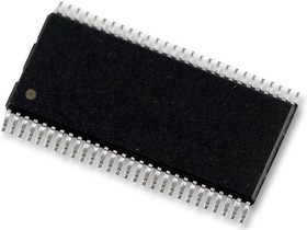
PCA9698DGG,512, Расширитель I/O, 40бит, 1 МГц, I2C, SMBus …The PCA9698DGG is a 40-bit Fm+ I²C-bus advanced I/O Port with RESET, OE and INT organized in 5 banks of 8-I/Os. At 5V supply voltage, the outputs are capable of sourcing 10mA and sinking 25mA with a total package load of 1A to allow direct driving of 40 LEDs. Any of the 40 I/O ports can be configured as an input or output. The PCA9698 is the first GPIO device in a new fast-mode Plus (Fm+) family. Fm+ devices offer higher frequency (up to 1MHz) and longer, more densely populated bus operation (up to 4000pF). The device is fully configurable: output ports can be programmed to be totem-pole or open-drain and logic states can change at either the acknowledge (bank change) or the stop command (global change), each input port can be masked to prevent it from generating interrupts when its state changes, I/O data logic state can be inverted when read by the system master.
• 64 Programmable slave addresses using 3 address pins
• Readable device ID (manufacturer, device type and revision)
• Low standby current
• Latch-up testing is done to JEDEC standard JESD78 which exceeds 100mA
 Личный кабинет


 Загрузка